Photoluminescence tool for concentration (AlGaN), LED characterization, layer thickness and Bow measurements
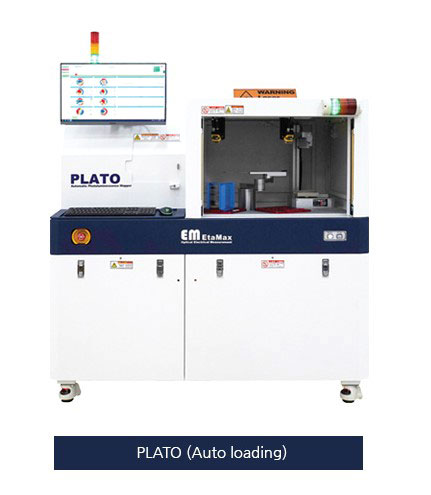
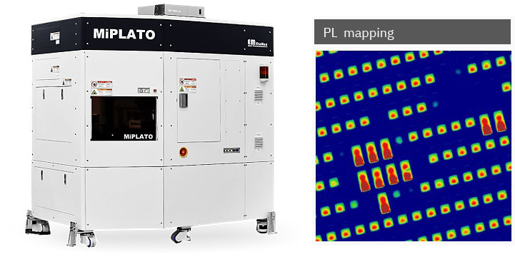
EUMETRYS, Associated with HORIBA - ETAMAX, distribute several tools for photoluminescence measurement. PLATO is a non-destructive mapping measurement system that uses PL(Photoluminescence) phenomenon. The photoluminescense analysis coupled with different laser sources can be used in multiple application:
The PLATO 200 and PLATO 300 can measure wafer from all sizes for Al contents in AlGaN layer, Thin-film thickness of GaN layer and even Bow measurement.
Eumetrys is the exclusive distributor in Europe for ETAMAX product line.
Do not hesitate to contact us to get a technical brochure by clicking here
EUMETRYS, Associated with HORIBA - ETAMAX, distribute several tools for photoluminescence measurement. PLATO is a non-destructive mapping measurement system that uses PL(Photoluminescence) phenomenon. The photoluminescense analysis coupled with different laser sources can be used in multiple application:
- GaN power devices
- AI composition in AIGaN layer
- VCSEL and NIR laser diode
- NIR for optical communications
- VCSEL DBR
- RF GAN
- LEDS
- Yellow PL
- POWER GAN
The PLATO 200 and PLATO 300 can measure wafer from all sizes for Al contents in AlGaN layer, Thin-film thickness of GaN layer and even Bow measurement.
Eumetrys is the exclusive distributor in Europe for ETAMAX product line.
Do not hesitate to contact us to get a technical brochure by clicking here