Eumetrys provides equipment and services for various applications in semiconductor and compound semiconductor industries. Optical metrology, particles inspection, and layer thickness measurement tools must be integrated in an innovating and challenging environment. That’s why, we take care to meet needs given by industrials and R&D laboratories thanks to our team of specialists.
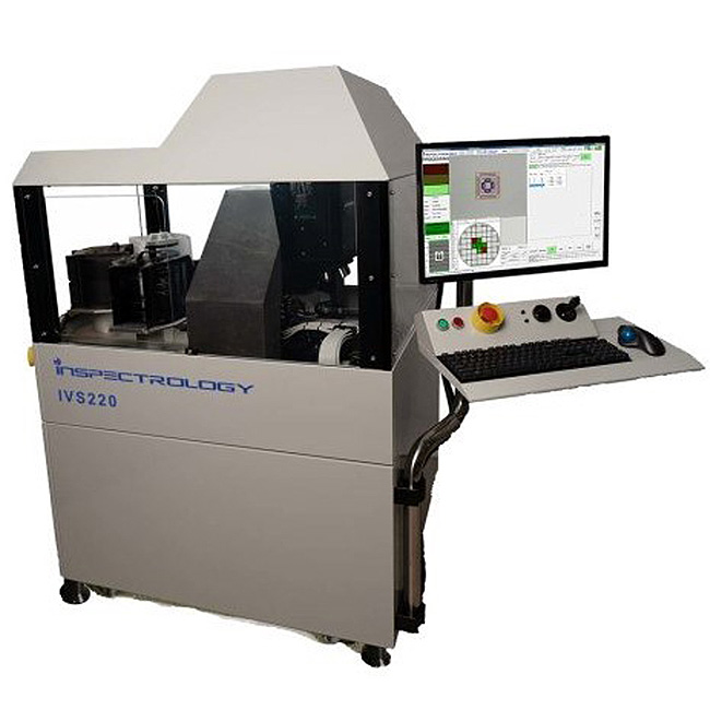
Eumetrys offer covers requirements of chips, MEMS, LED, waveguides, and substrates manufacturers. ONTO innovation IVS products line is designed to support lithography processes with an efficient optical metrology and limited costs. Overlay registration analysis allows stepper qualification and control as well as matching tests. Furthermore, ONTO innovation IVS products offer submicronic critical dimensions measurement (CD) especially 3D structure analysis.
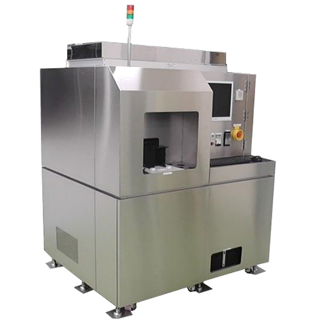
Our particles inspection equipment is used to control transparent and opaque wafer’s surface contamination. EPI or SiC filmed wafers inspection is very demanding and push to rise important technological challenges. YPI-MX YGK products combined to Eumetrys’ services win this bet and support compound semiconductors industrials.
Eumetrys offer covers requirements of chips, MEMS, LED, waveguides, and substrates manufacturers. ONTO innovation IVS products line is designed to support lithography processes with an efficient optical metrology and limited costs. Overlay registration analysis allows stepper qualification and control as well as matching tests. Furthermore, ONTO innovation IVS products offer submicronic critical dimensions measurement (CD) especially 3D structure analysis.
Our particles inspection equipment is used to control transparent and opaque wafer’s surface contamination. EPI or SiC filmed wafers inspection is very demanding and push to rise important technological challenges. YPI-MX YGK products combined to Eumetrys’ services win this bet and support compound semiconductors industrials.