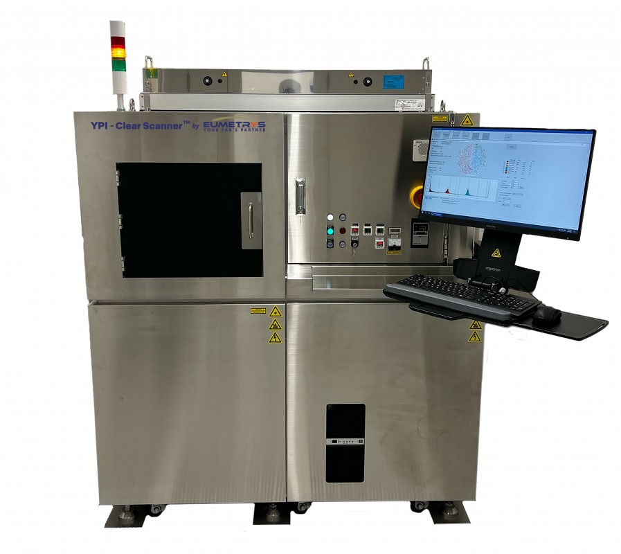
Wafer Surface Particle Scanner
Inspection for Compound & Transparent Wafers
High-Performance Inspection for Unpatterned Transparent and Opaque Wafers
Eumetrys delivers leading-edge solutions for surface inspection and particle detection on unpatterned wafers used in compound semiconductor fabrication. Our flagship system, the YPI – Clear Scanner™, is a versatile wafer surface particle scanner designed to detect submicron particles, haze, scratches, and area defects on a wide range of wafer types — from transparent and semi-transparent substrates to thin and bowed wafers.
In collaboration with YGK, a Japanese manufacturer with over 20 years of experience, Eumetrys provides exclusive global access to this advanced tool. The system plays a critical role in improving yield, cleanliness control, and defect prevention in high-value semiconductor production.
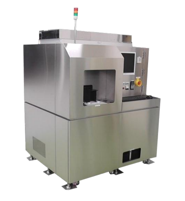
Turnkey particle inspection system for transparent and opaque substrates
YPI – Clear Scanner™: Flexible and Powerful Particle Inspection for Compound Wafers
Turnkey particle inspection system for transparent and opaque substrates
Eumetrys offers particle inspection equipment for transparent (SiC, GaN, Crystal, Sapphire…) and opaque substrates. The YPI tool range has the advantage of a low cost of ownership while being adaptable to customer needs, and notably allows for process and contamination control with measurements on EPI wafers or with SiC films.
In order to meet the needs of the semiconductor industry and share our support experience, Eumetrys has partnered with YGK and expanded its offering with efficient and versatile products. This Japanese firm has been present in the semiconductor industry for over 20 years and its primary goal is designing high-quality particle contamination analysis equipment. This partnership combines the performance of YGK products with the efficiency and responsiveness of Eumetrys' experts.
Transparent substrates benefit from innovative technology implemented on the YPI-MX-DC equipment. Inspect the particle contamination of your 2'' to 8'' SiC and GaN wafers. Fully customizable and affordable, this tool meets all expectations regarding the control of standard, translucent, transparent wafers or those with thin films.
The YPI-MX equipment is intended for the silicon semiconductor and compound semiconductor industries. It allows for contamination control of a wide variety of substrates such as Si, Crystal, Sapphire, LiNbO3, or LiTaO3 on all wafer sizes up to 8 inches.
Particle inspection for transparent substrates
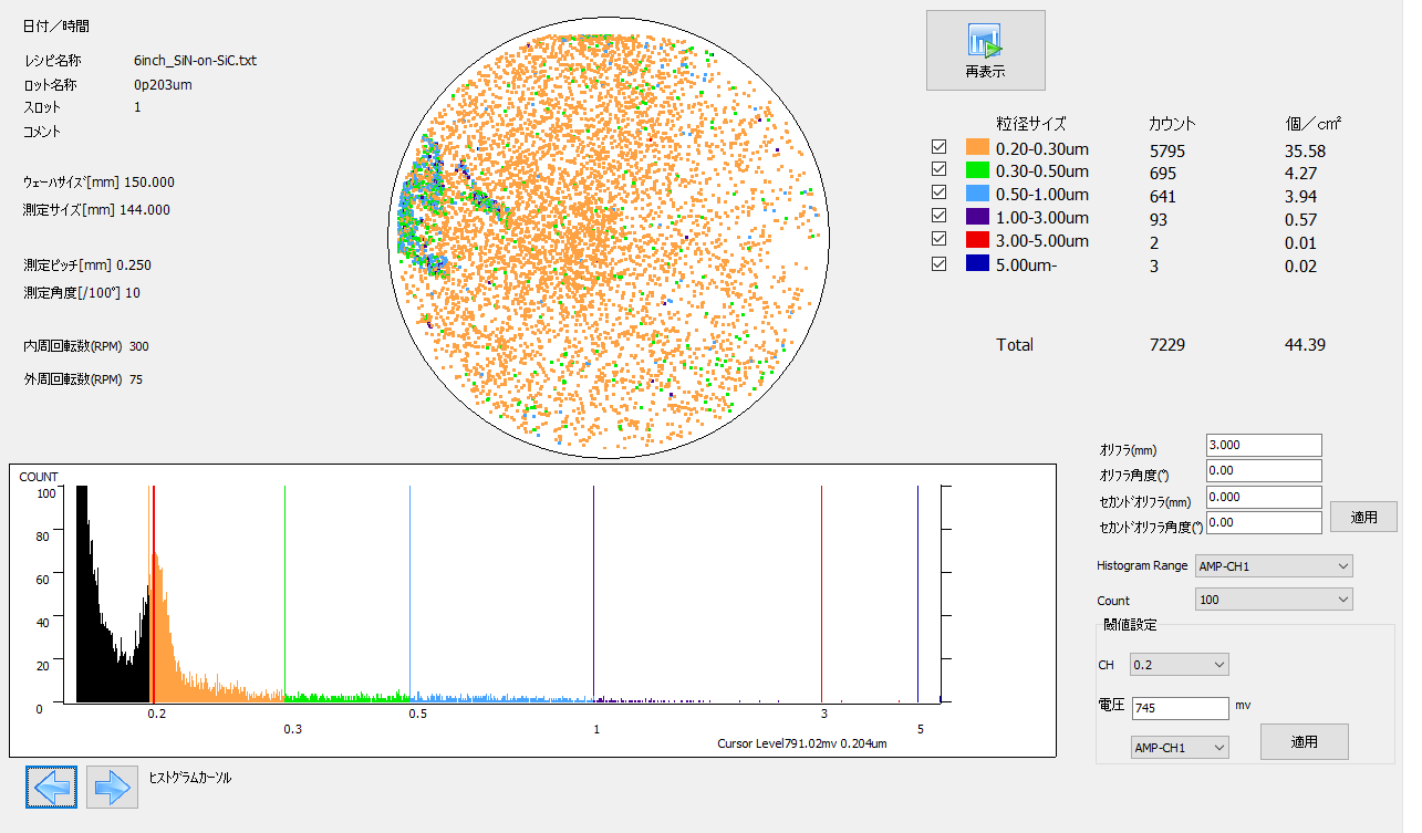
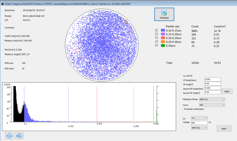
The YPI-MX-DC model detects particle contamination down to 0.1µm on transparent substrates. Operating on 2 to 8-inch wafers, it is capable of inspecting materials such as SiC and GaN. Its 355 nm wavelength laser facilitates work on substrates for the compound semiconductor industry.
For the most exotic applications, it is possible to double the number of optical heads. A second detector channel can be added to improve measurement accuracy.
This product is ideal for carrying out the following applications:
• Process control
• Wafer contamination control, notably those with thin films or EPI on SiC
• Equipment contamination control
• Polishing process control
• Incoming control of wafers from your suppliers
XY scanning allows for working on square wafers and substrates, and helical scanning is specialized for processing wafers.
The YPI-MX-DC, specialist in surface inspection of transparent substrates
The YPI-MX-DC can be equipped with a 355nm laser. This wavelength is ideal for inspecting transparent and translucent substrates, even those with thin films.
The YPI-MX-DC is equipped with a standard load port and a cassette-to-cassette handling robot. We also offer an optional second load port and a dual-paddle robot.
Particle inspection for opaque and transparent substrates
The YPI-MX model is capable of detecting particle contamination measuring 0.1 µm on a wide variety of substrates up to 8 inches. It performs measurements on Si, Crystal, Sapphire, LiNbO3, or LiTaO3 using its 405nm wavelength laser. It is possible to add a second optical head which improves measurement accuracy. The applications for this tool are varied.
• Process control
• Wafer contamination control, notably those with thin films or EPI on SiC
• Equipment contamination control
• Polishing process control
• Incoming control of wafers from your suppliers
The YPI-MX has another advantage. That is the ability to perform two types of scans: an XY scan and a helical scan. We recommend XY scanning for square wafers and substrates and helical scanning for round wafers or substrates.
YPI-MX, a versatile and customizable equipment
This technology detects particles down to 0.1 µm. Edge exclusion is standard and represents 3mm. The equipment is therefore designed for both standard and specific applications.
The tool has a standard load port and an automatic handling robot. The robot is capable of loading 2'' to 8'' wafers. Optionally, it is possible to add load ports and install a dual-paddle robot.