Automated optical metrology systems
Overlay registration and critical dimension measurement
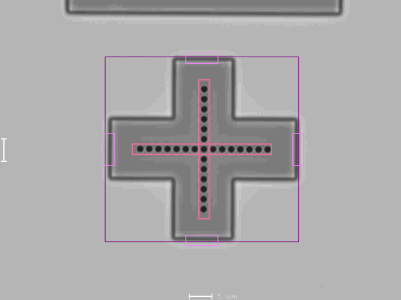
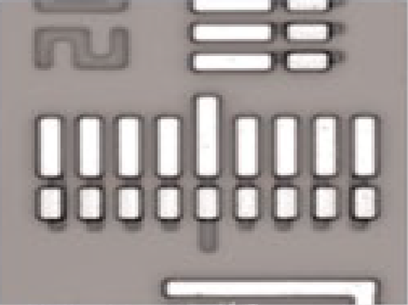
Turnkey IVS optical system for Critical Dimension (Line width) and layer alignment (Overlay Registration) measurements
EUMETRYS, EUropean METRology sYStem, is the service company supporting optical metrology systems for European semiconductor, compound semiconductor, MEMS, and LED factories.

Thanks to many years of expertise in optical measurement, EUMETRYS sells automated optical metrology systems and their spare parts, provides application support, maintenance, and delivers training to users (process and maintenance) for factories and laboratories of microelectromechanical systems (MEMS), semiconductors, compound semiconductors (GaAs, GaN, SiC, InP, Glass, Sapphire), and LEDs (Light Emitting Diodes).

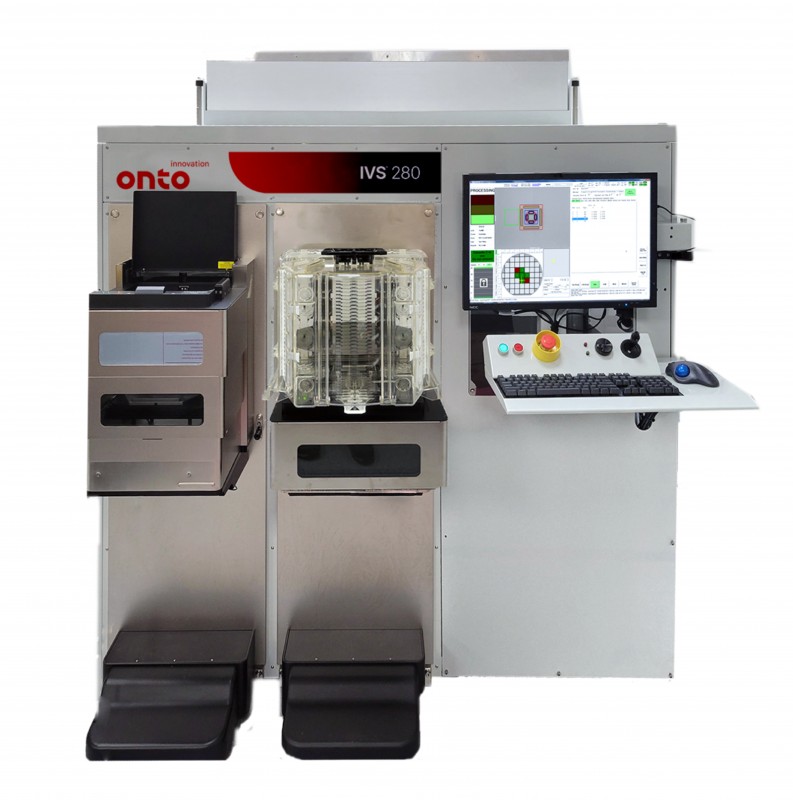
We offer the latest model from ONTO Innovation's R&D departments: the IVS 380. At the cutting edge of technology, the IVS380 incorporates innovations and features renowned for 40 years. Here you will find the product's technical specifications. The IVS380 system integrates the same technical data as the IVS220 (cassette-to-cassette tool, limited to 200mm substrates) or the IVS280 (OHT/E84 tool, limited to 200mm substrates). The IVS380 offers compatibility with 300mm wafers or a 200/300 hybrid version with OHT/E84 capability.

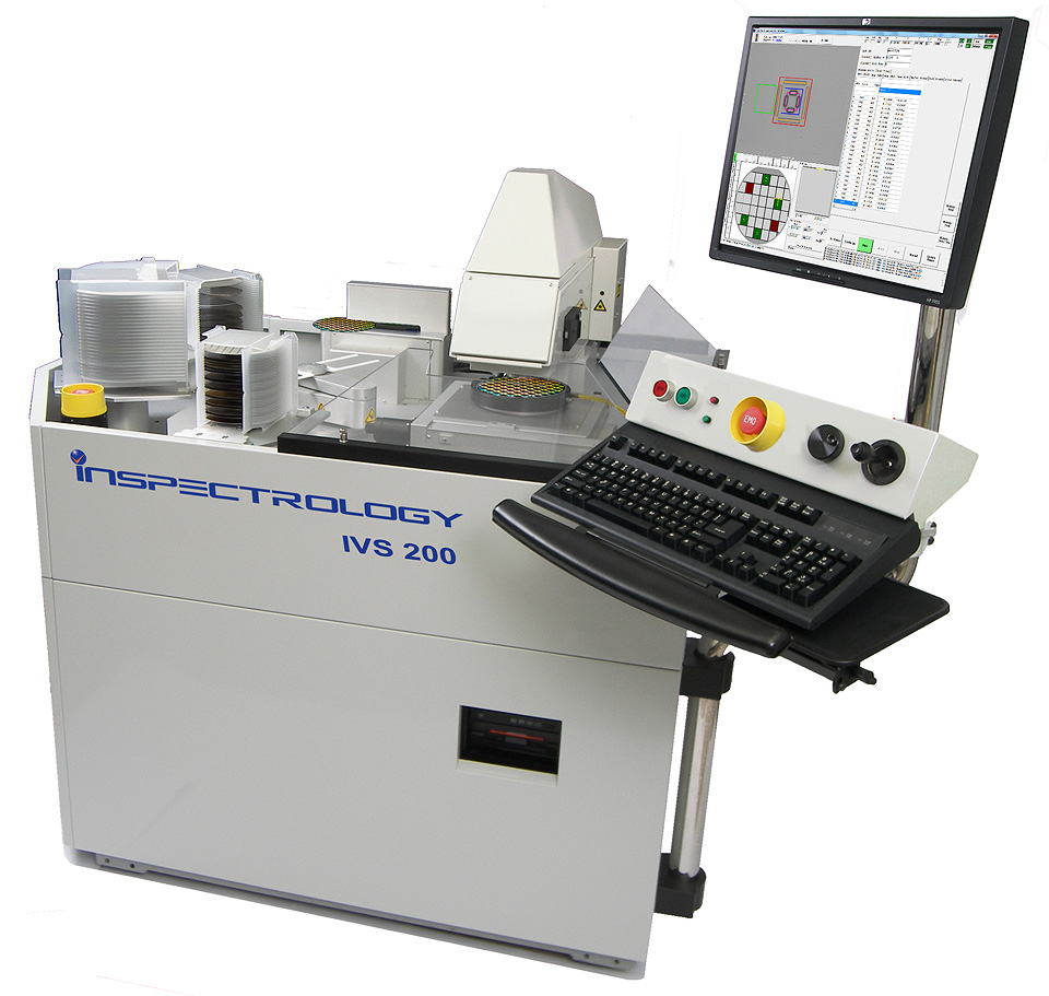
In order to meet each customer's needs and budgetary constraints, EUMETRYS is able to provide refurbished IVS1x or IVS200 tools and guarantee the performance of this tool proven by semiconductor manufacturers. Click here for more details.

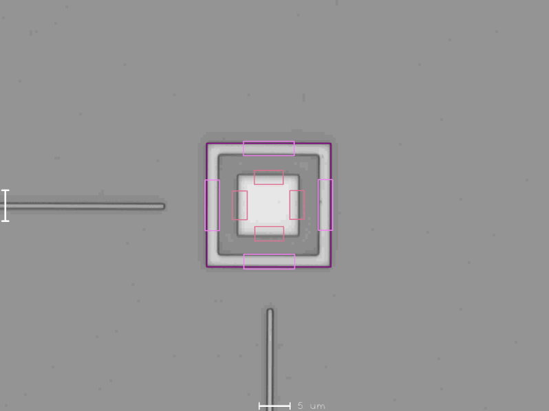
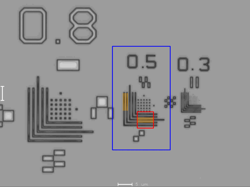
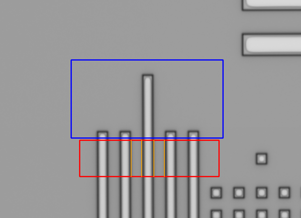
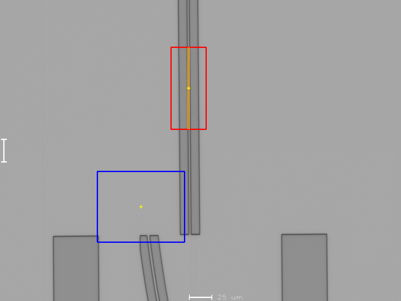
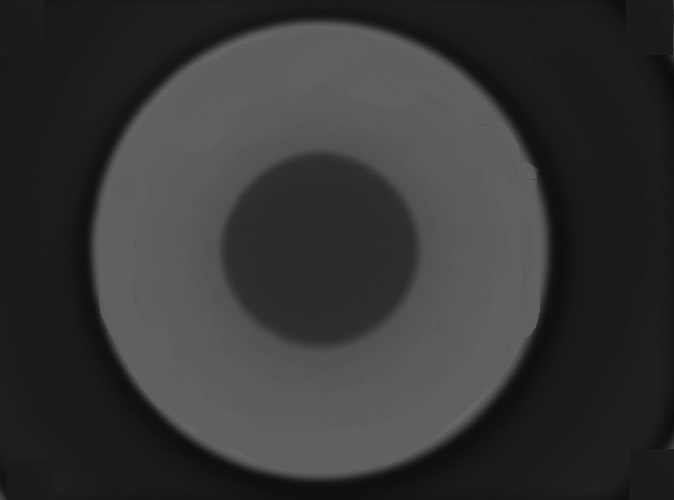
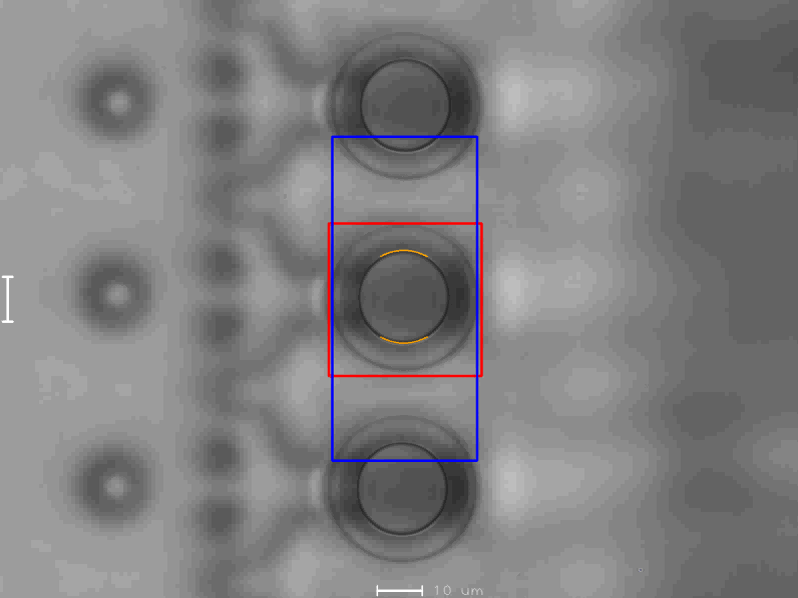
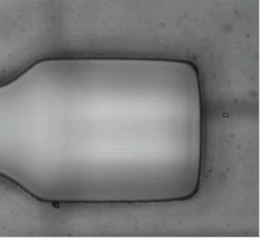
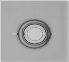
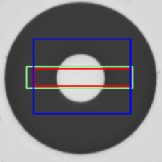
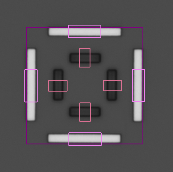
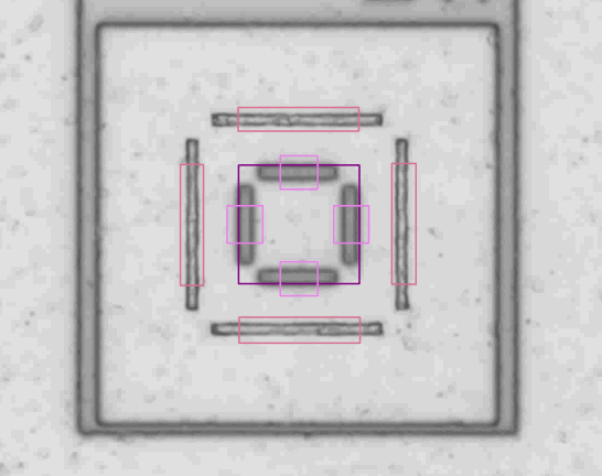
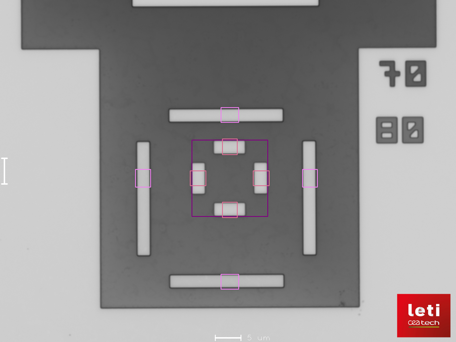
EUMETRYS is the exclusive distributor in Europe and Israel for the OEM equipment manufacturer ONTO Innovation for CD and Overlay measurement tools. The IVS are automatic optical measurement systems for Critical Dimensions and Layer Alignment.


ONTO innovation IVS 280 / 380

Eumetrys now sells the new IVS 280 and IVS 380 systems, a high-speed automated optical measurement tool at the forefront of metrology for 8'' wafers and below, and for 12'' Si or GaN/Si wafers.

The IVS 380 model offers the best cost per measurement for 65nm FEOL process node technologies in fabs producing 300mm wafers. With a record cycle time of 165 wafers per hour (TPUT), a 3 Sigma precision below 1 nanometer, and with 1 nanometer of TIS, the IVS 380 tool is designed to meet both advanced 90nm Front End technologies and the more agile needs of CD measurement, Via measurements, bump thickness for MEMS, and advanced wafer packaging, the most modern advanced metrology needs.

The system uses Image Based Overlay (IBO) imaging, and can measure critical dimensions (Critical Dimension - CD or Line Width - LW), alignment marks (Overlay registration), vernier-type layer alignments, VIA and bump diameters, heights, and even slopes for measuring all patterns drawn in photolithography under the resist layer. It is designed to qualify technological nodes down to 65nm for semiconductor fabs but also to meet the demand for flexibility from the compound semiconductor industries with several types of substrates as varied as SiC, InP, GaN, GaN-on-Si, Glass, Sapphire, and GaAs substrates.

The tool is based on the proven IVS 220 system and meets all the demands of our customers. From a reliable and renowned base, we have added high-technology elements such as the ETEL platform in order to push the limits of measurement speed and accuracy.

With the IVS380 tool, ONTO Innovation and Eumetrys support the industries and the ever-stricter requirements of their processes.


ONTO Innovation IVS 220 / IVS280 Systems (Formerly Inspectrology)


Eumetrys continues to offer the IVS 220 and IVS 280 systems; these are high-speed automated optical measurement tools at the forefront of metrology. The IVS 280 can, in addition to the IVS220, support E84 technology for loading via OHT or AGV.

The IVS 220 model offers the best cost per measurement for the most advanced technologies in fabs producing wafers up to 200mm. With a record cycle time of 165 wafers per hour (TPUT), a 3 Sigma precision below 1 nanometer, and with 1 nanometer of TIS, the IVS 220 tool is designed to meet modern advanced metrology needs. The IVS280 follows the same specifications but can also receive automated lot loading.

With the IVS220, IVS280, and IVS 380, Eumetrys and ONTO Innovation offer manufacturers various options to meet different configurations and resolve the ever-stricter requirements of their processes.


EUMETRYS sells a flexible and automatically loaded optical metrology system for the Semiconductor, MEMS, LED, power, and photonics industries

The IVS 220, IVS 280, and IVS 380 optical measurement tools are specialized in overlay registration measurements for photolithography stepper & scanner control and for critical dimension (CD) measurements.

The IVS220 and IVS280 tools are built to handle multiple types and sizes of substrates and wafers from 75mm to 200mm without any hardware changes to the system. The IVS380 tool can handle 200mm and 300mm substrates. All of them can measure transparent substrates as well as bonded wafers, again without any system modification or hardware pre-configuration.

The EUMETRYS team has many years of experience in the semiconductor world. We deliver an efficient solution to our customers who are concerned with maintaining their system's Mean Time Between Failures (MTBF) and UPTIME at the highest level. We work with many factories having only a single metrology line. This is also why we have minimized our response time as much as possible to minimize the Mean Time To Repair (MTTR).

EUMETRYS is the exclusive representative of Onto Innovation for the IVS product line in Europe and Israel. We sell the new IVS220, IVS280, and IVS380 models with the best cost-effectiveness ratio on the market for 300mm, 200mm, and smaller substrates.

Contact us for more information
 

Refurbished IVS 1x and IVS 200 models

Depending on customer needs and budgetary constraints, we offer second-hand systems: Warranty and specifications are maintained with the best Cost of Ownership (COO) on the market for this generation: IVS1x or IVS 200.

At Eumetrys, we believe that all customers deserve an efficient, relevant, and cost-controlled solution. This is why we decided to provide a second-hand system completely refurbished by our services.

We let you benefit from our expertise to remanufacture the IVS1x and IVS200 that we have produced over the years. Despite their obsolescence, we offer services including spare parts.

These tools are delivered with their original specifications, acceptance, training, and a 6-month warranty. They are fully supported by our services and by the brand's technical support.

The IVS1x models have demonstrated the best cost/effectiveness ratio. More than just a standard CD and overlay measurement tool, the IVS 1x offers a wide range of metrology algorithms allowing the measurement of various structures for semiconductors, compound semiconductors, MEMS, and LEDs. It is widely used in the telecom, power, and photonics industries.

This extremely flexible system allows the user to measure Overlay and CD in the same recipe.

The IVS 1x model offers great flexibility in terms of measurements and allows its use in both compound semiconductors and standard semiconductors even while cost-effectiveness is a key factor for your factory.

For the best price-quality ratio: IVS1x Contact us.


IVS BRAND CAPABILITIES

The possibilities of IVS
  • For transparent substrates, the IVS systems are equipped with a transparent alignment system based on innovative imaging. This allows measurements of transparent wafers and advanced technology substrates such as Glass, Quartz, GaN, GaAs, LiNbO3, InP, and SiC.
  • Critical dimension (CD) and layer alignment (Overlay) measurements in the same recipe for standard production monitoring: This tool is able to locate and measure CDs, Overlay, or other patterns inside the chip to meet production control needs.
  • From submicron CD or pitch measurements for advanced technologies up to large CD or pitch measurements thanks to powerful objectives going up to 150X.
  • New SiC / InP substrates: The IVS 220, IVS 280, and IVS380 systems are capable of measuring patterns on complex substrates thanks to their transparent measurement option used in the power, waveguide, and photonics industries and for VCSEL products. The IVS220 and IVS 280 systems are currently used by most Compound semiconductor manufacturers with large production volumes.
  • The IVS 380 System has been chosen by advanced Semiconductor manufacturers for deep layer thickness measurement for new advanced Wafer packaging techniques.
  • 3D structural measurement algorithm: MEMS structures metrology, CD, CD height, and VIA (thanks to circular fitting measurement capabilities) are regularly used by process engineers in charge of IVS systems. The software flexibility of the IVS1x, IVS 200, and IVS220/280 and 380 systems allows customers to perform control measurements on complex layers inside the chip or along the scribe line of the substrates.
  • LED, VCSEL, Laser structure measurements and Vias metrology: With the advent of new technologies, customer demand has evolved, and the IVS220 / IVS 280 and IVS380 systems have adapted accordingly. The tool offers a new Via measurement algorithm and new VCSEL opening measurement capabilities, for example.
  • Recognized Overlay measurement capability for Semiconductor processes down to 65nm: The IVS220 / 280 and 380 systems are cost-effective solutions for measuring alignment marks in complex layers and structures for processes down to 110nm. The IVS1x and IVS200 systems allow resolving technologies limited to 110nm.
  • Specific measurements of very large Overlays at LETI – Nano-Imprint Lithography (NIL)
  • Measurements of exotic Overlay patterns and Verniers: In new compound semiconductor productions, Overlay measurements do not always use standard SEMI features. The IVS200, IVS220, IVS280, and IVS380 systems allow for non-standard Overlay measurements such as cross-in-cross, verniers, and other exotic Overlay patterns.

For every customer request, our Applications team works to find a solution to meet it.
In-chip or monitoring of CD & overlay measurement in the same recipe – for standard production tracking
 
The tool is able to locate and measure CD, overlay or various patterns within the chip of your product for the production product control.
 

In-chip CD measurement
 

In-chip overlay registration measurement

From sub-micron CD or pitch measurements for advanced technology nodes to rather large CD or pitch measurements thank to a large objectives panel from 150X to 2.5X
 
For the various customer needs, the IVS200 system software is allowing the user’s to measure standard CD as well as sub-micron CD or pretty large CD up to the field of view size.
 

Sub micron CD or pitch measurement
 

Large CD or pitch measurement

New SiC / InP substrates
 
The IVS200 system is able to measure challenging patterns of new substrates using the transparent option for power, waveguides, photonics industries and VCSEL products
                         
The IVS200 system is currently in use in most compound semiconductor manufacturer with volume production requirement.
 

Ridge CD of photonics
 

Laser opening for VCSEL

Structural 3D measurement algorithm
 
Structural MEMs, CD, CD height and VIA metrology (thank to circle fitting measurement capabilities) are commonly is use for the IVS200 system users.
          
The versatility of the IVS200 software allows the customer to measure in-chip or inside the scribe line for various metrology control on challenging layers.
 

Challenging VIAs in chip
 

MEMs printer head pad

Structural LED, VCSEL / Laser, CD measurement and VIA metrology
 
On new technology, the customer measurement demand had changed and the IVS200 system has been developed accordingly. The tool offers new Via algorithm and new capabilities to measure VCSEL aperture for instance.
 

In-chip VIAs measurement
 

VCSEL aperture measurement

Strong proven overlay capability down to 110 nm semiconductor processes
 
The IVS200 system is the cost-effective solution for measuring overlay registration feature in advance layer challenging context as well as difficult structures down to 110 nm Process node.
 

TiN overlay capability
 

Semi standard overlay advance layer

Specific measurement of very large overlays at the LETI – NanoImprint Lithography (NIL)


Sub-micron CD or pitch measurement


Exotic overlay pattern measurement and Vernier
 
In the new compound semiconductor production, the overlay demand is not always using the SEMI standard feature target to measure the overlay.
         
The IVS200 system is allowing non-standard overlay feature measurement including (non-exhaustive list) cross in a cross, Vernier, …
 
For each customer demand our applications team is working to find a solution for the customer.
 

Exotic overlay pattern
 

Overlay Vernier