Non-patterned surface inspection for process monitoring on SiC, GaN, Si or glass Wafers
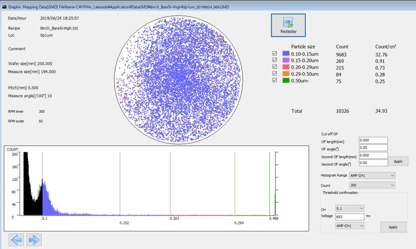
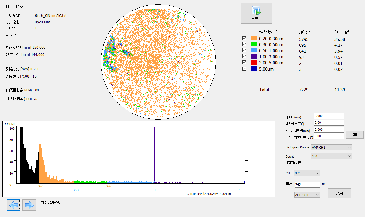
The YGK scanning tool can track particles at each process or cleaning steps. The key added value of the YGK scanning system is the capability to track particles deposited on wafers during the different part of the process as described down below. Particles can be measured on SiC (Silicon Carbide), GaN (Gallium Nitride), Si (Silicon) wafers thanks to specific hardware setup:
With different Scanning capabilities and parameters, the surface contamination analysis system can handle all types of wafers and provide you high quality results thanks to its fast acquisition time and optimized sensitivity.
The YGK scanning tool can track particles at each process or cleaning steps. The key added value of the YGK scanning system is the capability to track particles deposited on wafers during the different part of the process as described down below. Particles can be measured on SiC (Silicon Carbide), GaN (Gallium Nitride), Si (Silicon) wafers thanks to specific hardware setup:
- Process Monitoring: Can count the number of particles during the process of your production wafers. Results are presented by size. A calibration is made to improve the quantity and size accuracy of the detected particles
- Incoming check: Check the number of particles of your manufacturing incoming wafers
- Wafer Cleaning: Measure the number of particles and their size after each cleaning step
- Polishing Process: Wafers can be analyzed after being polished
- PWP test for process equipment: Particles per wafer pass can be monitored using the surface contamination analysis system
With different Scanning capabilities and parameters, the surface contamination analysis system can handle all types of wafers and provide you high quality results thanks to its fast acquisition time and optimized sensitivity.