Optical reflectometry for film thickness uniformity analysis
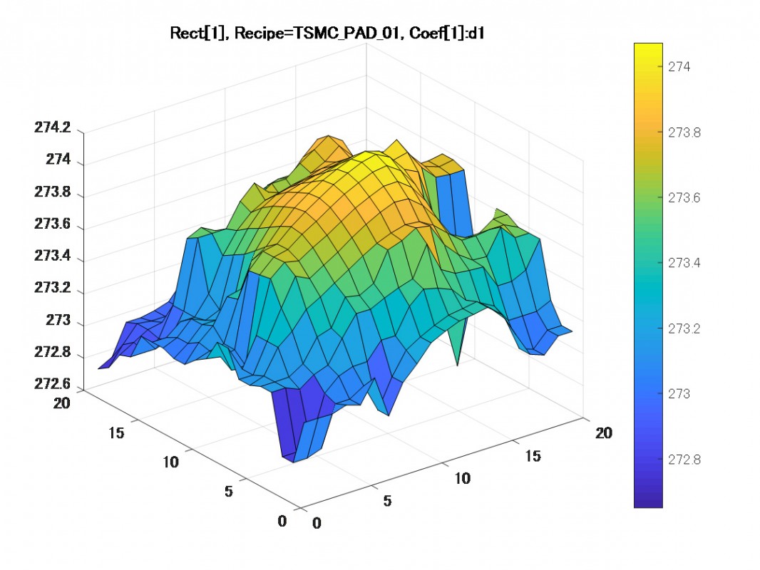
The EFiT-TT reflectometry tool can render in 3D the film characteristics. From film thickness distribution of SiO2 on Si to complex film porosity on low-K materials, the EFiT tabletop tool provides a 3D analysis in the field of view of the microscope. Films on glass, PET, silicon wafers and other can be analyzed within different field of view sizes provided by the tool. To analyse porous film, the film thickness monitor can measure the mixture ratio (density) and film thickness separately if the target layer has sufficient film thickness. Thanks to modeling capabilities, film thickness resolution is under 1 nm and the density resolution is under 1%.
Discover our offer by clicking here
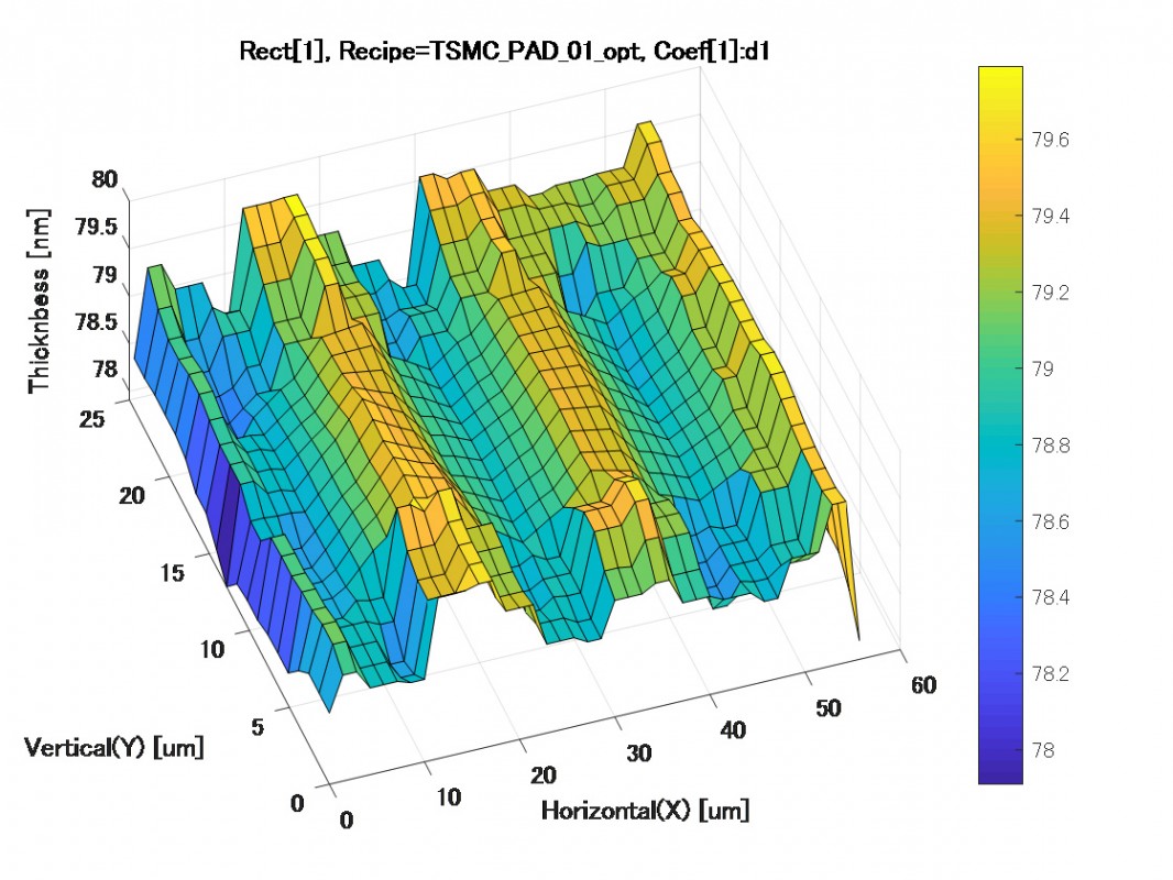